Circuit features
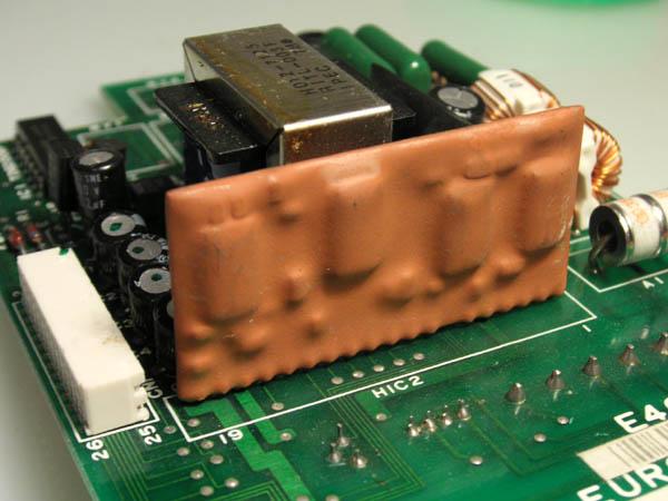
Hybrid integrated circuit is a circuit that concentrates the functional parts of all components in a circuit on a substrate, which can basically eliminate the auxiliary parts in the electronic components and the assembly between the components Voids and solder joints can improve the assembly density and reliability of electronic equipment. Due to this structural feature, the hybrid integrated circuit can be used as a distributed parameter network with electrical performance that is difficult to achieve with a discrete component network. Another feature of hybrid integrated circuits is to change the sequence, thickness, area, shape and properties of the three films of conductor, semiconductor and dielectric, and their lead positions to obtain passive networks with different properties.

Types of circuits
There are two commonly used film forming techniques for the manufacture of hybrid integrated circuits: screen printing sintering and vacuum film forming. The film made by the former technique is called thick film, and its thickness is generally above 15 microns, while the film made by the latter technique is called thin film, and the thickness ranges from several hundred to several thousand angstroms. If the passive network of the hybrid integrated circuit is a thick film network, it is called a thick film hybrid integrated circuit; if it is a thin film network, it is called a thin film hybrid integrated circuit. In order to meet the requirements of miniaturization and integration of microwave circuits, there are microwave hybrid integrated circuits. According to the concentration and distribution of component parameters, this circuit is divided into concentrated parameter and distributed parameter microwave hybrid integrated circuits. The structure of the lumped parameter circuit is the same as that of a general thick film hybrid integrated circuit, except that the component size accuracy is higher. The distributed parameter circuit is different. Its passive network is not composed of visually distinguishable electronic components, but is entirely composed of microstrip lines. The dimensional accuracy of the microstrip line is relatively high, so thin film technology is mainly used to manufacture distributed parameter microwave hybrid integrated circuits.
Basic process
In order to facilitate automated production and close assembly in electronic equipment, the manufacture of hybrid integrated circuits uses standardized insulating substrates. The most commonly used are rectangular glass and ceramic substrates. One or several functional circuits can be fabricated on a single substrate. The manufacturing process is to first manufacture membrane passive components and interconnections on the substrate to form a passive network, and then install semiconductor devices or semiconductor integrated circuit chips. The film-type passive network is manufactured by photolithography and film-forming methods. According to a certain process sequence on the substrate, conductors, semiconductors and dielectric films with various shapes and widths are manufactured. These layers are combined with each other to form various electronic components and interconnections. After the entire circuit is fabricated on the substrate, the lead wires are soldered, and when necessary, a protective layer is coated on the circuit, and finally sealed with a shell to become a hybrid integrated circuit.
Application development
The applications of hybrid integrated circuits are mainly analog circuits and microwave circuits, and they are also used in special circuits with higher voltage and higher current. For example, data conversion circuits in portable radio stations, airborne radio stations, electronic computers and microprocessors, digital-to-analog and analog-to-digital converters, etc. The application in the microwave field is particularly prominent.
Development trend
The development trend of hybrid integration technology is: ①Use multi-layer wiring and carrier tape soldering technology to assemble and interconnect monolithic semiconductor integrated circuits to achieve secondary Integration, production of complex multi-functional, high-density large-scale hybrid integrated circuits. ②The passive network develops to be denser, more precise and more stable, and the sensitive components are integrated in its passive network to create an integrated sensor. ③Develop high-power, high-voltage, and high-temperature hybrid integrated circuits. ④Improve film-forming technology to make the manufacturing process of thin-film active devices practical. ⑤Assemble micro-chip leadless components and devices with a substrate with interconnection lines to reduce the price of electronic equipment and improve its performance.
